
Cheaper, smaller specialist microscope invented in Australia could help create new materials or even quality-check new phones.
A microscope that fits in the palm of your hand could soon become a standard tool for generating high-resolution images of atoms, cells, and new materials. The new device opens up a range of applications in industry.
Researchers at the University of Newcastle, Australia, in collaboration with researchers at the University of Texas at Dallas, US, shrank an atomic force microscope to the size of a USB stick by miniaturising its core components to fit on a single silicon chip. Not only does this make the microscope smaller and cheaper, it also leads to improved performance.
Atomic force microscopes are a critical tool in the material sciences, but until now they usually take up a whole lab bench and cost as much as a quarter of a million dollars. They can generate a 3D image of almost any surface—plastic, biological or composite materials—down to the nanoscale or one billionth of a metre.
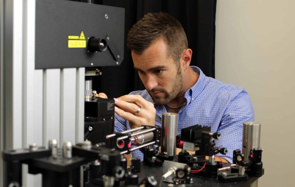
“What’s novel about our design is that all the moving mechanical and sensing parts are now built into one tiny chip; we’ve gotten rid of the measurement laser and other bulky parts,” says Dr Michael Ruppert, who lead-authored the first publication of this design, and is now a lecturer in Mechatronics at the University of Technology Sydney.
“At the core of the microscope is a tiny cantilever with a nanoscopic needle at one end – like the arm and needle on a conventional record player,” says Dr Ruppert. “The needle is as long as a human hair is wide, and the end of the tip is only about 100 times larger than a single atom.”
As the tiny needle feels its way over the surface of a sample, vibrations of the cantilever plot minute changes across the surface of the sample. From those vibrations, the instrument can generate a kind of topographic map of a sample, showing the peaks and troughs of the surface at the atomic scale.
The current research efforts concentrate on making the cantilever chips smarter and more powerful. The new designs are set to reduce the costs of atomic force microscopes significantly – down from hundreds of thousands of dollars for today’s conventional microscopes to just thousands of dollars. In the process, Dr Ruppert is talking to industrial partners in instrument manufacturing around the world about incorporating the technology into existing microscopes and further developing the manufacturing process.
“The great thing about this design is that it’s adaptable and scalable. We can look at a particular research problems or industry applications where fast imaging could help and re-design the chip specifically for that role.”
One application currently in development is upgrading a room-size instrument which scans electronic components of phones and computers to detect quality issues during manufacturing. The next generation of this instrument would use a bank of the microscope chips working in parallel and therefore drastically increasing throughput and efficiency.
The microscopes could also play an important role in the development of new materials – particularly polymers and semiconductors – by allowing scientists and manufacturers to “see” at the nanoscale, if a new material has a desired property, for instance the ability to repel water or generate charge due to the photovoltaic effect.
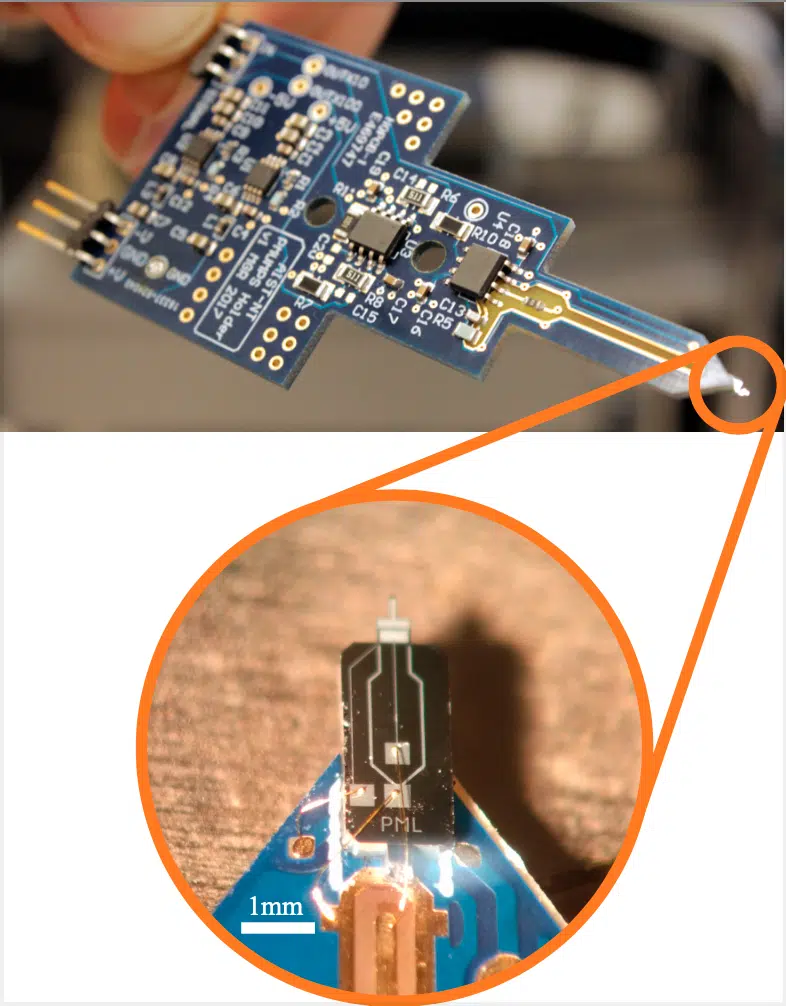
Sensor with the tiny cantilever structure at the tip.


 Fresh Science is on hold for 2022. We will be back in 2023.